- 您现在的位置:买卖IC网 > Sheet目录1993 > DS1123LE-100+ (Maxim Integrated Products)IC DELAY LINE 256TAP 16-TSSOP
DS1123L
3.3V, 8-Bit, Programmable Timing Element
_____________________________________________________________________
9
effect on power-up. The most flexibility when using par-
allel mode occurs when the delay is being controlled
by a microprocessor.
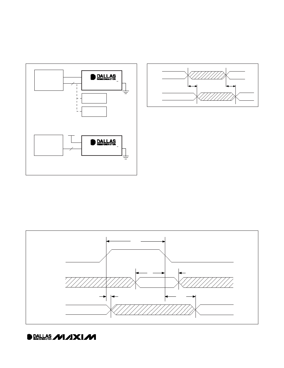
There are two common parallel interface implementa-
tions used to control the DS1123L using a microproces-
sor (see Figure 2). LE can be used to latch the data
from the microprocessor, which allows the data bus to
be shared with other peripherals, or LE can be tied
high, which causes the DS1123L to adjust its delay
immediately following a change to the parallel inputs.
For each configuration, a settling time (tEDV or tPDV) is
required after an adjustment is made before the input
signal is accurately delayed according to the new set-
ting. Figures 3 and 4 show the timing required for these
implementations.
Using the Serial Programming Interface
The 3-wire serial interface is enabled by connecting P/S
to VCC. Serial mode operates similar to a shift register.
When LE is set at a high logic level, it enables the reg-
ister and CLK clocks the data, D, into the register one
bit at a time starting with the most significant bit. After
all 8 bits are shifted into the DS1123L, LE is pulled low
to end the data transfer and activate the new value. A
settling time (tEDV) is required after LE is pulled low
before the signal delay meets its specified accuracy. A
timing diagram for the serial interface is shown in
Figure 6. The 3-wire interface also has an output (Q)
that can be used to cascade multiple 3-wire devices,
and it can be used to read the current value of the
devices on the bus.
LE
P0-P7
P/S
8
MICROPROCESSOR
ADDITIONAL
PERIPHERAL
ADDITIONAL
PERIPHERAL
A) SHARING THE PARALLEL INTERFACE
WITH ADDITIONAL PERIPHERALS
MICROPROCESSOR
8
B) A PARALLEL INTERFACE DEDICATED
TO A DS1123L
VCC
DS1123L
LE
P0-P7
P/S
DS1123L
Figure 2. Parallel Interface Options for DS1123L
PREVIOUS VALUE
PARALLEL
INPUTS
P0–P7
DELAY
TIME
NEW VALUE
PREVIOUS VALUE
tPDX
tPDV
Figure 3. Nonlatched Parallel Timing Diagram
ENABLE
(LE)
PREVIOUS VALUE
NEW VALUE
tEW
tDSE
tEDX
tEDV
tDHE
PARALLEL
INPUTS
PO–P7
DELAY
TIME
Figure 4. Latched Parallel Timing Diagram
发布紧急采购,3分钟左右您将得到回复。
相关PDF资料
DS1124U-25+T
IC DELAY LINE 256TAP 10-USOP
DS1135LU-300/T&R
IC DELAY LINE 300NS 8-USOP
DS1135Z-12/T&R
IC DELAY LINE 12NS 8-SOIC
DS1181LE+
IC CLOCK MOD SS 8-TSSOP
DS1243Y-120
IC NVSRAM 64KBIT 120NS 28DIP
DS1244W-120IND
IC NVSRAM 256KBIT 120NS 28DIP
DS1248Y-70IND
IC NVSRAM 1MBIT 70NS 32DIP
DS1251WP-120+C02
IC NVSRAM 34PWRCP
相关代理商/技术参数
DS1123LE-200
功能描述:延迟线/计时元素 Programmable 3.3V 8 Bit Timing Element RoHS:否 制造商:Micrel 功能:Active Programmable Delay Line 传播延迟时间:1000 ps 工作温度范围: 封装 / 箱体:QFN-24 封装:Tube
DS1123LE-200+
功能描述:延迟线/计时元素 Programmable 3.3V 8 Bit Timing Element RoHS:否 制造商:Micrel 功能:Active Programmable Delay Line 传播延迟时间:1000 ps 工作温度范围: 封装 / 箱体:QFN-24 封装:Tube
DS1123LE-25
功能描述:延迟线/计时元素 Programmable 3.3V 8 Bit Timing Element RoHS:否 制造商:Micrel 功能:Active Programmable Delay Line 传播延迟时间:1000 ps 工作温度范围: 封装 / 箱体:QFN-24 封装:Tube
DS1123LE-25+
功能描述:延迟线/计时元素 Programmable 3.3V 8 Bit Timing Element RoHS:否 制造商:Micrel 功能:Active Programmable Delay Line 传播延迟时间:1000 ps 工作温度范围: 封装 / 箱体:QFN-24 封装:Tube
DS1123LE-50
功能描述:延迟线/计时元素 Programmable 3.3V 8 Bit Timing Element RoHS:否 制造商:Micrel 功能:Active Programmable Delay Line 传播延迟时间:1000 ps 工作温度范围: 封装 / 箱体:QFN-24 封装:Tube
DS1123LE-50+
功能描述:延迟线/计时元素 Programmable 3.3V 8 Bit Timing Element RoHS:否 制造商:Micrel 功能:Active Programmable Delay Line 传播延迟时间:1000 ps 工作温度范围: 封装 / 箱体:QFN-24 封装:Tube
DS1123LS-200
功能描述:延迟线/计时元素
RoHS:否 制造商:Micrel 功能:Active Programmable Delay Line 传播延迟时间:1000 ps 工作温度范围: 封装 / 箱体:QFN-24 封装:Tube
DS1123LS-25
功能描述:延迟线/计时元素
RoHS:否 制造商:Micrel 功能:Active Programmable Delay Line 传播延迟时间:1000 ps 工作温度范围: 封装 / 箱体:QFN-24 封装:Tube